Consainsights logo
Mail Us
Background Image

Indium Phosphide Wafer Market Report

Indium Phosphide Wafer Market by Product (Bulk Wafers, Epitaxial Wafers, Substrates), Application (Telecommunications, Aerospace and Defense, Healthcare, Consumer Electronics, Sensor Technologies), and Region – Analysis on Size, Share, Trends, COVID-19 Impact, Competitive Analysis, Growth Opportunities and Key Insights from 2023 to 2030.

01 Executive Summary

Indium Phosphide Wafer Market Size & CAGR

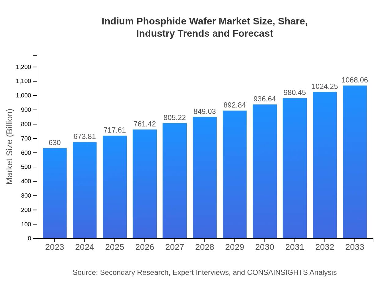
The global Indium Phosphide Wafer market size is projected to reach USD 630 million by 2023, with a Compound Annual Growth Rate (CAGR) of 5.3% during the forecast period from 2023 to 2030. The forecasted growth rate signifies a steady increase in demand for Indium Phosphide wafers across various industries, including telecommunications, aerospace, and defense.

COVID-19 Impact on the Indium Phosphide Wafer Market

The COVID-19 pandemic has had a significant impact on the Indium Phosphide Wafer market, disrupting supply chains and causing fluctuations in demand. Lockdowns and restrictions imposed to curb the spread of the virus resulted in delays in manufacturing and shipment of Indium Phosphide wafers, affecting market growth. However, as economies gradually reopen and industries resume operations, the market is expected to recover and witness growth in the post-pandemic period.

Indium Phosphide Wafer Market Dynamics

The Indium Phosphide Wafer market is driven by the increasing demand for high-performance semiconductor materials in various applications, such as optical communication, radar systems, and solar cells. The unique properties of Indium Phosphide, including high electron mobility and low noise characteristics, make it an ideal material for advanced electronic devices. However, the market faces challenges such as price fluctuations of raw materials and intense competition from other semiconductor materials.

Segments and Related Analysis of the Indium Phosphide Wafer market

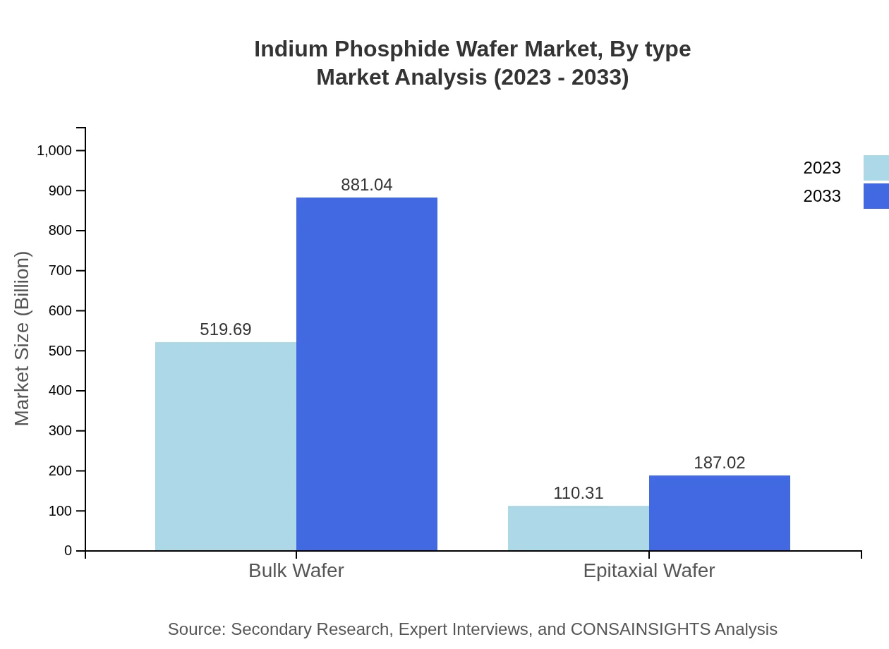
The Indium Phosphide Wafer market can be segmented based on wafer diameter, application, and end-user industry. By wafer diameter, the market is divided into 2-inch, 3-inch, 4-inch, 6-inch, and others. In terms of application, the market includes wireless communication, optical communication, photonic devices, and others. The end-user industries for Indium Phosphide wafers include telecommunications, aerospace and defense, healthcare, and others.

Indium Phosphide Wafer market analysis report by Region

Asia Pacific Indium Phosphide Wafer market report

The Asia Pacific region is a key market for Indium Phosphide wafers, driven by the growing demand for smartphones, 5G technology, and fiber-optic communication. Countries like China, Japan, and South Korea have a strong presence in the semiconductor industry, contributing to the market growth in the region.

South America Indium Phosphide Wafer market report

South America has a developing semiconductor industry, with Brazil and Argentina emerging as key players in the market. The demand for Indium Phosphide wafers in the region is driven by the increasing adoption of advanced technologies in communication and healthcare sectors.

North America Indium Phosphide Wafer market report

North America is a mature market for Indium Phosphide wafers, with the presence of prominent semiconductor companies and research institutes. The region leads in technological advancements in telecommunications, aerospace, and defense, driving the demand for high-quality semiconductor materials like Indium Phosphide.

Europe Indium Phosphide Wafer market report

Europe is a significant market for Indium Phosphide wafers, with countries like Germany, France, and the UK playing a crucial role in semiconductor manufacturing. The demand for high-performance electronic devices and communication systems in Europe drives the growth of the Indium Phosphide Wafer market in the region.

Middle East and Africa Indium Phosphide Wafer market report

The Middle East and Africa region have a growing demand for Indium Phosphide wafers, fueled by investments in telecommunications infrastructure and renewable energy projects. Countries like UAE, Saudi Arabia, and South Africa are investing in advanced semiconductor technologies, driving the market growth in the region.

Indium Phosphide Wafer market analysis report by Technology

The Indium Phosphide Wafer market can be analyzed based on epitaxial growth technology, lithography technology, and etching technology. Epitaxial growth technology is essential for the production of high-quality Indium Phosphide wafers, while lithography and etching technologies are used for patterning and structuring semiconductor devices.

Indium Phosphide Wafer market analysis report by Product

The Indium Phosphide Wafer market offers products such as bare wafers, epi-ready wafers, and patterned wafers. Bare wafers are used for research and development purposes, while epi-ready wafers are ready for epitaxial growth. Patterned wafers have specific designs for different semiconductor applications.

Indium Phosphide Wafer market analysis report by Application

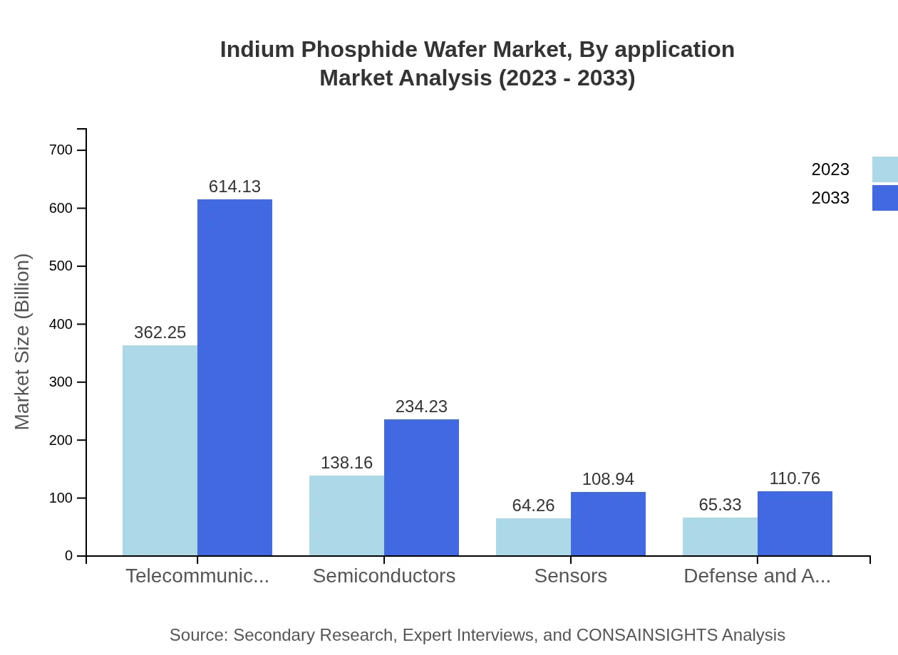
Indium Phosphide wafers find applications in optical communication, wireless communication, photonic devices, and solar cells. Optical communication applications include fiber-optic networks, while wireless communication applications cover 5G technology and satellite communication. Photonic devices utilize Indium Phosphide wafers for laser diodes and LED manufacturing.

Indium Phosphide Wafer market analysis report by End-User

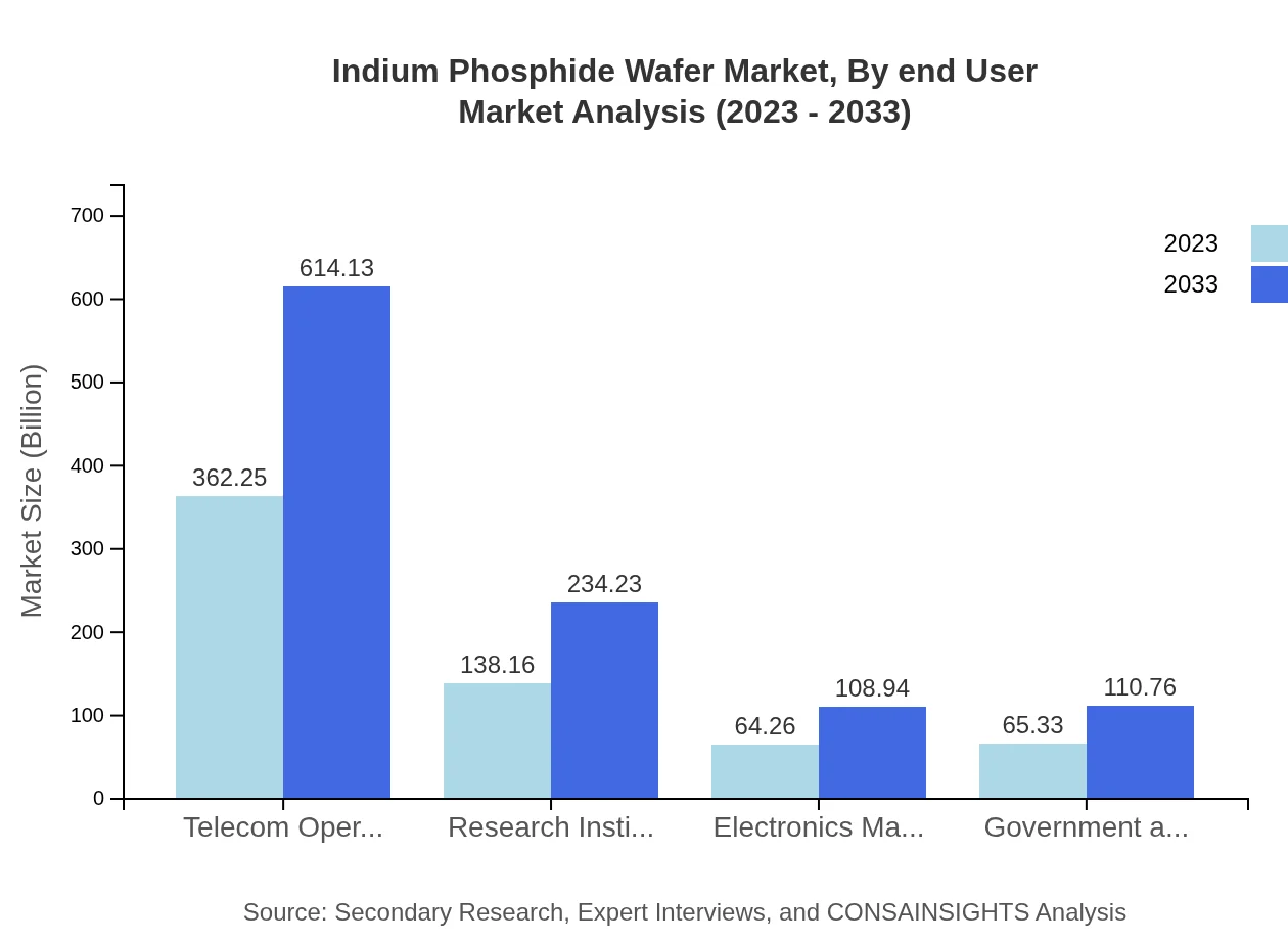
The end-users of Indium Phosphide wafers include telecommunications companies, aerospace and defense industries, healthcare sector, and research institutions. Telecommunications companies use Indium Phosphide wafers for high-speed data transmission, while aerospace and defense industries employ them in radar systems and satellite communication. The healthcare sector utilizes Indium Phosphide wafers for medical imaging applications.

Key Growth Drivers and Key Market Players of Indium Phosphide Wafer market

Key growth drivers for the Indium Phosphide Wafer market include the increasing demand for high-speed communication systems, the rise of 5G technology, and the growing adoption of photonics in various applications. The market players operating in the Indium Phosphide Wafer market include:

  • IQE PLC
  • WIN Semiconductors Corp.
  • Sumitomo Electric Industries
  • II-VI Incorporated
  • Lumentum Holdings Inc.

Indium Phosphide Wafer market trends and future forecast

The Indium Phosphide Wafer market is witnessing trends such as the increasing adoption of Indium Phosphide in 5G infrastructure, the development of integrated photonics solutions, and the advancements in epitaxial growth techniques. The future forecast for the Indium Phosphide Wafer market includes a continued growth trajectory driven by the expansion of telecommunications networks, the deployment of Internet of Things (IoT) devices, and the emergence of new applications in healthcare and automotive industries.

Recent happenings in the Indium Phosphide Wafer Market

1. IQE PLC announced a strategic partnership with a leading telecommunications company to supply Indium Phosphide wafers for the development of 5G infrastructure.

2. WIN Semiconductors Corp. introduced a new line of epi-ready Indium Phosphide wafers with enhanced performance for photonic applications.

3. Sumitomo Electric Industries collaborated with a research institution to develop advanced laser diodes using Indium Phosphide materials.

02 Research Methodology

Our research methodology entails an ideal mixture of primary and secondary initiatives. Key steps involved in the process are listed below:

  • Step 1. Data collection and Triangulation

    This stage involves gathering market data from various sources to ensure accuracy and comprehensiveness.

  • Step 2. Primary and Secondary Data Research

    Conducting in-depth research using both primary data (interviews, surveys) and secondary data (reports, articles) to gather relevant information.

  • Step 3. Data analysis

    Analyzing and interpreting the collected data to identify patterns, trends, and insights that can inform decision-making.

  • Step 4. Data sizing and forecasting

    Estimating the size of the market and forecasting future trends based on the analyzed data to guide strategic planning.

  • Step 5. Expert analysis and data verification

    Engaging subject matter experts to review and verify the accuracy and reliability of the data and findings.

  • Step 6. Data visualization

    Creating visual representations such as charts and graphs to effectively communicate the data findings to stakeholders.

  • Step 7. Reporting

    Compiling a comprehensive report that presents the research findings, insights, and recommendations in a clear and concise manner.

Data collection and Triangulation

The foundation is meticulous data gathering from multiple primary and secondary sources through interviews, surveys, industry databases, and publications. We critically triangulate these data points, cross-verifying and correlating findings to ensure comprehensiveness and accuracy.

Primary and Secondary Data Research

Our approach combines robust primary research discussion with industry experts and an exhaustive study of secondary data sources. A comprehensive analysis of published information from credible databases, journals, and market research reports complements direct interactions with industry stakeholders and key opinion leaders.

Data analysis

With a wealth of data at our disposal, our seasoned analysts meticulously examine and interpret the findings. Leveraging advanced analytical tools and techniques, we identify trends, patterns, and correlations, separating signal from noise to uncover profound insights that shed light on market realities.

Data sizing and forecasting

Armed with a profound understanding of market dynamics, our specialists employ robust statistical models and proprietary algorithms to size markets accurately. We go a step further, harnessing our predictive capabilities to forecast future trajectories, empowering clients with foresight for informed decision-making.

Expert analysis and data verification

Our research findings undergo a rigorous review by a panel of subject matter experts who lend their deep industry knowledge. This critical analysis ensures our insights are comprehensive and aligned with real-world dynamics. We also meticulously verify each data point, leaving no stone unturned in our pursuit of accuracy.

Data visualization

To unlock the true potential of our research, we employ powerful data visualization techniques. Our analysts transform complex datasets into intuitive visuals, including charts, graphs, and interactive dashboards. This approach facilitates seamless communication of key insights, enabling stakeholders to comprehend market intricacies at a glance.

Reporting

The final step is providing detailed reports that combine our in-depth analysis with practical advice. Our reports are designed to give clients a competitive edge by clearly explaining market complexities and highlighting emerging opportunities they can take advantage of.

03 Market Overview

Market Definition and Scope
Market Segmentation
Currency
Forecast
Assumptions

Market Definition and Scope

The Indium Phosphide wafer market refers to the segment of the semiconductor industry that focuses on the production, distribution, and application of Indium Phosphide (InP) wafers, which are critical for high-speed and high-frequency electronics.

Indium Phosphide, recognized for its superior electronic properties, is primarily utilized in optoelectronic devices, including lasers, photodetectors, and high-frequency transistors, marking a substantial scope within various industries such as telecommunications, aerospace, and consumer electronics.

This market encompasses both the manufacturing processes of these wafers and the technological advancements enhancing their performance, thus providing a comprehensive view of the market dynamics that influence pricing, demand, and innovation.

Understanding the scope also involves awareness of regional variations, regulatory frameworks, and economic factors contributing to market growth and the potential barriers faced by manufacturers and suppliers.

Overall, the Indium Phosphide wafer market is poised for growth as its applications expand, driven by cutting-edge developments in communications technology and quantum computing.

Market Segmentation

The Indium Phosphide wafer market can be segmented based on several criteria including application, end-use industry, and geography, each offering distinct insights into market trends and consumer behavior.

By application, the market is categorized into optoelectronics, high-speed electronics, and other segments, with optoelectronics holding a significant share due to its critical role in laser and LED technologies.

In evaluating end-use industries, telecommunications, defense, and automotive sectors exhibit the highest demand for Indium Phosphide wafers, reflecting the material's capability in facilitating advancements in fiber optics and military communications.

Geographically, the market can be divided into North America, Europe, Asia-Pacific, and the Rest of the World, where regions like Asia-Pacific are expected to witness rapid growth, driven by increasing manufacturing activities and technological innovation.

This segmentation allows stakeholders to tailor their strategies effectively by addressing specific market niches and leveraging opportunities within high-demand applications.

Currency

The financial transactions and market valuation within the Indium Phosphide wafer market are typically conducted in US Dollars (USD), providing a standardized currency for global trade.

Using USD facilitates easier comparison and understanding of market performances across different regions and currencies, thus enhancing transparency for investors and stakeholders.

Currency fluctuations may impact pricing strategies and profit margins, making it vital for companies to manage currency risks through hedging and strategic financial planning.

Furthermore, the currency in which transactions occur affects the market dynamics influenced by international trade policies, tariffs, and economic conditions prevalent in participating countries.

Forecast

Forecasts for the Indium Phosphide wafer market indicate a positive growth trajectory, with estimates suggesting a compound annual growth rate (CAGR) exceeding industry averages in the coming years.

Key factors driving this growth include surging demand for high-speed communication technologies and the expansion of optical networks, which require advanced materials like Indium Phosphide for performance improvement.

Emerging applications in sectors such as quantum computing and automotive electronics further enhance the market's forecast, as these fields demand high-efficiency materials capable of operating under stringent technical specifications.

Market analysis indicates that investment in research and development will play a crucial role in sustaining this growth, as innovations lead to more effective manufacturing processes and enhanced product offerings tailored to specific applications.

Overall, the comprehensive market forecast signifies the vital role of Indium Phosphide wafers in future technological advancements, reinforcing their importance in various emerging industries.

Assumptions

Key assumptions underpinning the Indium Phosphide wafer market analysis include the continuous growth of the telecommunications industry, which is expected to drive demand for high-performance semiconductor components.

It is also assumed that technological advancements will persist, leading to increased efficiency and a reduction in production costs of Indium Phosphide wafers, making them more accessible to a wider range of applications.

Additionally, the analysis presumes stable economic conditions globally, which would support investment and expansion in sectors that utilize Indium Phosphide wafers, thereby sustaining market demand.

Moreover, it is assumed that regulatory frameworks will evolve to support innovation within the semiconductor industry while maintaining safety and quality standards essential for consumer trust.

These assumptions collectively shape the strategic outlook for the Indium Phosphide wafer market, guiding stakeholders in their decision-making processes as they navigate this dynamic landscape.

04 Market Dynamics

Market Drivers
Market Restraints
Market Opportunities
Market Challenges

Market Drivers

The indium phosphide wafer market is primarily driven by the increasing demand for high-speed communication systems, where indium phosphide offers superior performance in optoelectronic devices.

Furthermore, the growth in data centers and telecommunication infrastructure has necessitated the utilization of high-performance semiconductors, further propelling the demand for indium phosphide wafers.

Advancements in technology, particularly in the fields of photonics and optoelectronics, are creating opportunities for innovative applications that leverage the unique properties of indium phosphide wafers.

The rising trend of integrating advanced materials into electronic devices, especially for applications like laser diodes and photodiodes, is significantly contributing to the market's growth.

Another factor includes the solid investments in research and development for enhancing the efficiency and reducing the costs of manufacturing indium phosphide wafers, which is expected to attract more players into the market.

Market Restraints

Despite the positive market outlook, the indium phosphide wafer market faces certain restraints, including high manufacturing costs, which can impede some companies from entering this sector due to the need for substantial initial investments.

Additionally, the availability of alternative materials, such as silicon, which can be cheaper and more widely produced, poses a direct competition threat to indium phosphide wafers, potentially limiting market expansion.

The complexity associated with the fabrication process of indium phosphide wafers adds to the operational challenges, as specialized equipment and skilled workforce are crucial for production.

Environmental regulations concerning the sourcing and usage of indium might also restrict overall production capabilities, influencing the pricing and availability of these wafers in the market.

Lastly, the volatility in the supply chain of raw materials needed for production, especially in the backdrop of political or environmental disruptions, remains a significant concern for market players.

Market Opportunities

With the continuous scaling of electronic devices and the internet of things (IoT), there presents a significant opportunity for indium phosphide wafers in developing high-efficiency, miniature components suited for these applications.

The rise of 5G technology is another opportunity for indium phosphide wafers, as they are critical for developing high-speed broadband infrastructure and integrating advanced wireless communication components.

Moreover, the growing adoption of renewable energy technologies, such as solar cells and photonic sensors, highlights the potential for indium phosphide in the clean energy sector, marking a clear route for market expansion.

Investments in automotive electronics, especially in electric vehicles and autonomous driving technologies, present another burgeoning frontier for indium phosphide wafers, where high-performance sensors and communication devices are essential.

Finally, global collaborations and partnerships aimed at advancing semiconductor research could lead to breakthroughs that enhance the performance and applications of indium phosphide wafers, thus expanding their market reach.

Market Challenges

The indium phosphide wafer market encounters several challenges, with one of the most pressing issues being the high cost of production, which impacts the pricing strategy and overall marketability of these wafers.

Furthermore, the lack of standardization in wafer specifications can lead to complexities in application, as different industries may require tailored solutions that can complicate manufacturing processes.

Supply chain disruptions due to geopolitical tensions or trade policies can also pose a threat to the stable availability of indium phosphide, which might affect long-term contracts and relationships with customers.

Additionally, the specialized nature of indium phosphide applications creates a limited customer base, which can be a risk factor, as dependencies on few clients can impact revenue stability during market fluctuations.

Finally, the need for highly skilled technicians and scientists in the semiconductor field creates a talent gap that could hinder the innovative capacity of companies looking to develop and implement new technologies involving indium phosphide wafers.

06 Regulatory Landscape

Overview of Regulatory Framework
Impact of Regulatory Policies on Market Growth

Overview of Regulatory Framework

The regulatory framework governing Indium Phosphide wafers is critical in ensuring the efficient and safe production, distribution, and utilization of these materials in various high-tech applications. Indium Phosphide (InP) is essential in the semiconductor industry, especially for applications in telecommunications, optics, and high-frequency electronics. Given its significance, a robust regulatory environment helps to foster innovation while safeguarding public health and the environment.

Regulatory bodies, including the U.S. Environmental Protection Agency (EPA), the European Chemicals Agency (ECHA), and various national and international standardization organizations, play a role in establishing the guidelines that govern how Indium Phosphide is sourced, manufactured, and disposed of. These regulatory frameworks are designed to address potential hazards associated with the raw materials required for InP production, such as indium and phosphorus, which can have toxicological effects if not handled appropriately.

Moreover, regulations will often vary based on the global landscape, with different countries adopting distinct approaches to manage the risks associated with the semiconductor industry and its materials. In many cases, these discrepancies can create challenges for manufacturers who operate on a global scale. Therefore, understanding the nuances of local regulation is crucial for compliance, market entry, and competitive advantage.

Another vital component of the regulatory landscape includes the prevailing environmental legislation that may impact manufacturing operations. Compliance with laws such as the Clean Air Act or the Resource Conservation and Recovery Act in the U.S. can dictate how companies manage emissions or waste products derived from the production of Indium Phosphide wafers. Non-compliance can lead to severe penalties and harm a company's reputation in the market.

Finally, the rapid technological advancements in semiconductor manufacturing often outpace regulatory updates. Thus, it is vital for regulators to continuously evaluate and adjust their frameworks to ensure they remain relevant and effective in addressing new challenges and opportunities presented by technological innovation in the Indium Phosphide sector.

Impact of Regulatory Policies on Market Growth

The impact of regulatory policies on the market for Indium Phosphide wafers is a multifaceted issue that encompasses economic, environmental, and technological dimensions. Firstly, regulatory frameworks can significantly affect market entry for companies wishing to produce or utilize Indium Phosphide. Strict regulatory requirements can act as a barrier to entry, hence, limiting competition and innovation.

However, while stringent regulations may seem like a challenge, they can also lead to higher quality standards, ultimately benefiting the end-users. For instance, regulations that enforce high levels of safety and environmental responsibility may require companies to adopt advanced manufacturing technologies and processes, which could increase operational costs in the short term. Nevertheless, these investments can lead to more efficient production methods and improved product reliability, which, in turn, can enhance a company’s standing in the market.

Furthermore, regulatory policies also affect the pricing structure of Indium Phosphide wafers. Compliance with environmental and safety regulations often necessitates additional expenses for manufacturers, which may lead to increased prices for end-users. Conversely, a well-structured regulatory environment that supports research and development can spur innovation, which may help to lower prices in the longer term as new cost-effective methods of production are developed.

Another significant aspect of how regulatory frameworks influence market growth is their ability to shape consumer confidence and market demand. When companies adhere to strict guidelines and demonstrate a commitment to ethical production processes, they cultivate trust among consumers and stakeholders. This increased consumer confidence can subsequently lead to higher demand for Indium Phosphide wafers, particularly in sectors like telecommunications, where reliability is paramount.

07 Impact of COVID-19 on the Artificial Intelligence Market

Short-term and Long-term Implications
Shift in Market Dynamics and Consumer Behavior

Short-term and Long-term Implications

The onset of the COVID-19 pandemic brought about immediate disruptions across various industries, including the Indium Phosphide wafer market. In the short term, manufacturing facilities faced temporary closures and reduced operational capacities due to health protocols, supply chain interruptions, and workforce shortages. As a result, production rates plummeted, leading to delays in delivering products to customers. This immediate impact was felt keenly, as many companies struggled to adapt to the changing environment, with some reporting substantial losses.

In addition to disruptions in production, the demand landscape for Indium Phosphide wafers also shifted significantly. Industries that primarily relied on these wafers, such as telecommunications and semiconductor manufacturing, saw a sharp decline in demand due to reduced consumer spending and postponed projects. The uncertainty surrounding the pandemic led to cautious spending behaviors, with many firms opting to delay or scale back their investments in new technologies, further exacerbating the challenges faced by wafer manufacturers.

However, as the world began to adapt to the pandemic, the long-term implications of COVID-19 on the Indium Phosphide wafer market began to emerge. The increasing reliance on digital infrastructure, driven by remote work and online services, bolstered demand for advanced communication technologies, which in turn invigorated the Indium Phosphide sector. Even as businesses reeled from the pandemic's immediate effects, a growing recognition of the need for robust connectivity solutions hinted at potential growth opportunities within the market.

Furthermore, the long-term effects of COVID-19 have prompted companies to rethink their operational strategies. There is now a significant emphasis on supply chain resilience, which is leading businesses to diversify their supplier networks and invest in localized production capabilities. Such strategic shifts are likely to enhance the sustainability of the Indium Phosphide wafer market and ensure it can better withstand future disruptions, whether caused by pandemics or other global uncertainties.

In summary, while the immediate impacts of COVID-19 on the Indium Phosphide wafer market were largely negative, the situation has also potentially spurred positive transformations in the industry that may herald a return to growth in the long run. Investment in new technologies and a focus on supply chain resiliency are key trends that could shape the future of this market, reflecting a critical adaptation to the challenges posed by the pandemic.

Shift in Market Dynamics and Consumer Behavior

The COVID-19 pandemic has significantly shifted market dynamics and consumer behavior in the Indium Phosphide wafer sector. In the early stages of the pandemic, the initial disruptions resulted in a contraction of demand from various end-user industries, leading to a decline in overall sales. This abrupt change forced manufacturers and suppliers to rethink their business models and strategies to remain competitive in an increasingly volatile landscape.

As the pandemic progressed, a noticeable shift occurred in the demand for advanced technologies, particularly in sectors such as telecommunications and data centers. The surge in remote working and online education necessitated enhanced communication capabilities, leading to increased investments in infrastructure that utilizes Indium Phosphide technology. As a result, manufacturers and suppliers witnessed a gradual recovery in demand, which began to reshape the market dynamics favorably.

Moreover, consumer behavior has significantly evolved due to the pandemic. The greater reliance on high-speed internet and connectivity has led consumers to prioritize swift and effective solutions, driving new demand patterns in the Indium Phosphide wafer market. Enterprises are now seeking high-performance components for their technology stacks, shifting focus from cost-cutting measures to quality and efficiency, which directly benefits manufacturers providing superior Indium Phosphide wafers.

These shifting dynamics have encouraged companies to innovate and differentiate their offerings more aggressively. The competition within the Indium Phosphide wafer market has intensified, prompting businesses to invest in research and development to create advanced solutions that address the growing need for speed and reliability in digital communications. Consequently, this focus on innovation is likely to yield a diverse array of new products that can better meet changing consumer expectations.

In conclusion, the impact of COVID-19 on the Indium Phosphide wafer market has resulted in substantial shifts in market dynamics and consumer behavior. While initial disruptions presented significant challenges, the pandemic has simultaneously accelerated the demand for advanced technologies and encouraged innovation within the industry. This evolution signifies a dual landscape of challenges and opportunities that could redefine the Indium Phosphide wafer market in the years to come.

08 Porter's Five Forces Analysis

Bargaining Power of Suppliers
Bargaining Power of Buyers
Threat of New Entrants
Threat of Substitutes
Competitive Rivalry

Bargaining Power of Suppliers

The bargaining power of suppliers in the Indium Phosphide wafer market is a critical factor that influences the overall supply chain dynamics. The suppliers of indium and phosphorous, the key materials used to produce Indium Phosphide wafers, possess significant power due to the limited number of raw material suppliers available. These materials are not only specialized but are also subject to fluctuations in availability and price, making the suppliers' ability to dictate terms fairly high.

Moreover, the production of Indium Phosphide wafers is technically complex, and suppliers who provide necessary high-purity raw materials have a competitive edge. The dependency on these specialized suppliers can lead to increased bargaining power as wafer manufacturers might face difficulty in switching to alternative suppliers without incurring substantial costs.

Additionally, the concentration of suppliers in regions with rich deposits of indium puts further pressure on wafer manufacturers. If suppliers choose to raise prices or impose unfavorable terms, it could directly impact the cost structure of manufacturers, reducing their profit margins. Manufacturers might need to establish long-term contracts or partnerships with suppliers to ensure a stable supply and negotiate better terms.

On the other hand, large manufacturers with significant purchasing power can negotiate better deals and reduce the influence of suppliers. However, smaller manufacturers often struggle with supply chain negotiations. This disparity in size and influence can affect competitive strategies within the market.

In summary, the bargaining power of suppliers in the Indium Phosphide wafer market is notably high, driven by the specificity of raw materials, limited supplier options, and the technical complexity of production. Wafer manufacturers must continuously assess their supplier relationships and seek to mitigate risks associated with supplier power through strategic alliances and diversified sourcing.

Bargaining Power of Buyers

The bargaining power of buyers in the Indium Phosphide wafer market is shaped by several factors, including the number of available suppliers, the level of differentiation among products, and the financial strength of the buyers themselves. Given the specialized nature of Indium Phosphide wafers, buyers often seek specific qualities and characteristics that cater to niche applications such as high-frequency electronics and optoelectronics.

Large-scale electronic manufacturers and semiconductor firms are typically the key buyers in this market. Their substantial purchasing volumes grant them considerable leverage when negotiating prices and terms with wafer manufacturers. As these buyers often engage in long-term contracts for consistency in supply, they can dictate market conditions, directly influencing pricing strategies and production schedules.

Furthermore, the increasing competition among suppliers has also empowered buyers. As more companies enter the Indium Phosphide wafer market, buyers find themselves with more options, which can drive prices down. Buyers are more likely to switch suppliers if they perceive better quality or lower prices elsewhere, compelling manufacturers to focus on quality and customer service to retain their client base.

In addition, technological advancements and the continuous evolution of the semiconductor industry mean buyers are often seeking the latest innovations in material properties and product performance. This demand pushes suppliers to consistently improve their offerings, thereby increasing the bargaining power of buyers who expect high-performance wafers at competitive prices.

In conclusion, the bargaining power of buyers in the Indium Phosphide wafer market is significant, primarily influenced by the size and purchasing power of consumers, the competitive landscape, and the demand for product differentiation. As buyers continue to seek cost-effective and innovative solutions, wafer manufacturers must adapt their strategies to meet these expectations while safeguarding their margins.

Threat of New Entrants

The threat of new entrants in the Indium Phosphide wafer market is influenced by several factors that determine market accessibility and competitive dynamics. One of the primary barriers to entry is the high capital requirement associated with establishing production facilities. The manufacturing process for Indium Phosphide wafers involves advanced technologies and equipment, necessitating heavy investment which can deter potential new players lacking access to substantial financial resources.

Moreover, the technical expertise required to produce high-quality Indium Phosphide wafers adds another layer of complexity. New entrants must possess not only the necessary funding but also a deep understanding of semiconductor physics and advanced manufacturing processes. This need for specialized knowledge acts as a significant barrier to entry, favoring established firms with experience and proven capabilities in the market.

The regulatory landscape also plays a crucial role in hindering new entrants. Compliance with quality standards and environmental regulations can be daunting for startups, and failure to meet such criteria can result in legal setbacks or financial penalties. Established companies usually have well-developed procedures for navigating these regulatory requirements, putting newcomers at a disadvantage.

Additionally, brand loyalty and established relationships between existing manufacturers and their clients further protect incumbents from new competition. Long-standing contracts and client trust can be difficult for new entrants to break into, as customers are often hesitant to switch suppliers, particularly in industries where quality and reliability are critical.

In summary, the threat of new entrants in the Indium Phosphide wafer market is relatively low due to high capital investment, technical complexity, regulatory requirements, and established client relationships. These barriers ensure that only well-prepared and adequately funded firms can realistically enter the market, serving to maintain the competitive landscape dominated by existing players.

Threat of Substitutes

The threat of substitutes for Indium Phosphide wafers is a crucial aspect to analyze, as it can significantly impact pricing strategies, market share, and overall demand. Substitutes refer to alternative materials or technologies that can perform similar functions as Indium Phosphide in applications like high-frequency communications, optoelectronics, and laser technology. Some of the most common substitutes include Gallium Arsenide (GaAs) and Silicon (Si).

Gallium Arsenide, for instance, is widely used in the semiconductor industry, particularly in applications requiring high efficiency and performance. As an established substitute, GaAs offers similar electronic properties, making it a formidable competitor to Indium Phosphide. Manufacturers might opt for GaAs if they seek cost savings or specific technical advantages, such as better performance in certain conditions.

Furthermore, advancements in research and material science could lead to the development of New Semiconductor materials that might outpace Indium Phosphide and traditional substitutes. Innovations in silicon-based technologies, such as Silicon Carbide (SiC) and other emerging materials, can pose a threat as they might quickly gain acceptance in the market if they demonstrate superior performance or cost-efficiency compared to existing options.

Another factor influencing the threat of substitutes is the evolving needs of consumers. As industries progress and require enhanced performance levels or lower costs, the incentive to switch to alternatives increases. If substitutes can meet or exceed the performance of Indium Phosphide wafers while offering better pricing or availability, manufacturers would gravitate towards switching suppliers.

In conclusion, while there exists some level of threat from substitutes in the Indium Phosphide wafer market, their potential impact largely relies on technological advancements, customer preferences, and specific application requirements. Manufacturers need to continuously monitor the competitive landscape, assess the performance of substitutes, and innovate to maintain a competitive edge.

Competitive Rivalry

The competitive rivalry within the Indium Phosphide wafer market is intense and shaped by several factors, including the number of players in the industry, the rate of industry growth, and the differentiation of products and services. With a growing demand for high-performance materials in electronics, more companies are entering the market, which raises competition levels as firms strive to capture market share.

Many established firms have significant market power due to their prolonged business presence, advanced manufacturing capabilities, and established distribution channels. This competitive advantage allows them to offer better prices or superior products, forcing newer entrants or smaller players to adopt more aggressive marketing tactics and pricing strategies to attract clients.

Moreover, continuous innovations and advancements in technology further heighten the rivalry as companies invest heavily in research and development to improve product quality and performance characteristics. Firms that can successfully develop unique features or superior materials often gain a significant competitive edge, leading to a race to innovate among industry players.

The increasing price competition is also a noteworthy element of rivalry, particularly among similar product offerings where differentiation might be minimal. Companies often resort to price reductions to attract customers or secure contracts, which can lead to reduced profit margins and financial stress across the industry as a whole.

In conclusion, competitive rivalry in the Indium Phosphide wafer market is robust, driven by numerous market players, technological advancements, and intense price competition. To thrive in this environment, companies must focus on innovation, build strong customer relationships, and differentiate their offerings to maintain a sustainable competitive advantage.

09 Key Insights and Findings

Market Analysis
Key Drivers
Market Challenges
Future Outlook
Competitive Landscape

Market Analysis

The Indium Phosphide wafer market is experiencing significant growth, driven by the increasing demand for high-performance electronics and photonics. With advancements in telecommunications, particularly in fiber optics and optical communications, the requirement for Indium Phosphide wafers continues to rise. These materials are known for their superior electronic properties, making them ideal for high-speed electronic devices and laser diodes.

Estimations suggest that the market will see a steady growth rate over the next few years. This growth can largely be attributed to the expanding use of Indium Phosphide in data communications, especially as the demand for high-bandwidth communication systems increases. As industries shift towards more integrated solutions requiring faster computing speeds and better thermal management, Indium Phosphide emerges as a front-runner due to its efficiency in such applications.

Moreover, the growing trend towards miniaturization in electronics supports the expansion of the Indium Phosphide wafer market. Smaller and more powerful devices are becoming the norm, and Indium Phosphide is pivotal in enabling these designs due to its favorable material properties. This is also reflected in various sectors, including consumer electronics, aerospace, and automotive industries, where performance standards are constantly on the rise.

The market's global landscape reveals a significant focus on R&D, with many players investing heavily to innovate and optimize Indium Phosphide wafer production processes. Such efforts intend to reduce manufacturing costs while enhancing the quality and reliability of the end products. This competitive edge is essential in a market characterized by rapid technological advances and high customer expectations.

Additionally, strategic collaborations among industry players, research institutions, and universities represent a growing trend aimed at unlocking new applications and improving wafer designs. This collaborative approach helps to foster an environment where innovative solutions can flourish, paving the way for novel technologies built on the foundation of Indium Phosphide materials.

Key Drivers

The Indium Phosphide wafer market is propelled by several key drivers that are influencing its growth trajectory. First and foremost, the telecommunication industry's surging demand for high-speed data transfer solutions is a critical factor. With the advent of 5G technology, the need for efficient, high-capacity materials has escalated, placing Indium Phosphide wafers in a strategic position to meet these challenges. As a result, manufacturers are ramping up production to cater to this evolving demand.

Secondly, the automotive sector's transition towards electrification and advanced driver-assistance systems (ADAS) is prompting an increased need for advanced semiconductor materials. Indium Phosphide wafers are well-suited for these applications due to their high electron mobility and effective thermal conductivity. This market segment continues to expand, driven by consumer demands for safer and smarter vehicles, which will bolster the market for Indium Phosphide wafers significantly.

Moreover, the proliferation of IoT (Internet of Things) devices plays a substantial role. As connectivity expands across various consumer and industrial applications, the requirement for reliable and fast communication channels becomes paramount. Indium Phosphide wafers are integral in delivering the performance needed for these IoT devices, supporting the ongoing digital transformation across numerous industries.

Another significant driver is the sustained investment in research and development across the global semiconductor industry. Companies are keen to explore the capabilities of Indium Phosphide for future applications, such as quantum computing and photonics-based technologies. These investments are expected to yield advancements in wafer technology, effectively stimulating market growth and diversifying application opportunities.

Lastly, growing environmental concerns are pushing industries toward greener alternatives. Indium Phosphide's capability to support energy-efficient processes offers manufacturers a chance to adhere to stricter regulations while remaining competitive and innovative. As sustainability becomes a priority, the wafers' role in promoting eco-friendly technologies could further amplify the market's growth potential.

Market Challenges

Despite the promising growth prospects of the Indium Phosphide wafer market, several challenges remain that could hinder progress. The primary concern is the high production cost associated with Indium Phosphide wafers. Compared to other semiconductor materials like silicon, the intricate fabrication processes and raw material costs can deter potential manufacturers from investing in this technology. Companies must balance quality and cost to compete in an increasingly price-sensitive market.

Another challenge is the limited supply of raw materials. Indium, the critical component of Indium Phosphide, is not abundantly available, and its extraction impacts the wafer production chain. Supply chain interruptions can occur due to geopolitical factors or market volatility, which must be navigated carefully by industry players. These disruptions can lead to increased prices and uncertainty in the market.

Moreover, technological barriers exist in the widespread adoption of Indium Phosphide wafers. While the material excels in performance metrics, the existing infrastructure in many industries is heavily reliant on silicon-based technologies. Transitioning to Indium Phosphide requires significant capital investments for equipment and processes, making it less attractive for some companies. This shift may take longer than anticipated due to the sunk costs in existing silicon technologies.

Furthermore, the market faces competition from alternative materials that offer similar or better performance characteristics. For instance, advancements in other semiconductor technologies, such as gallium nitride (GaN), could divert attention and investment away from Indium Phosphide. Therefore, maintaining a competitive edge will require ongoing innovation and adaptation from developers in the industry.

Last but not least, the regulatory landscape presents challenges as well. Industries such as telecommunications and automotive are subject to stringent regulations regarding safety and environmental impacts. Navigating these regulations can be complex, particularly when introducing new materials into existing systems. Companies must invest time and resources to ensure compliance, further complicating market dynamics.

Future Outlook

The future outlook for the Indium Phosphide wafer market appears favorable, with significant opportunities for growth in various sectors. As technology continues to evolve, the need for high-efficiency, high-performance materials is becoming increasingly critical. Indium Phosphide's unique properties, such as high electron mobility and low thermal resistance, position it as a leading candidate for next-generation applications in electronics and optics.

Forecasts indicate that demand from the telecommunications sector will remain strong, particularly with the rollout of 5G and beyond. The push for global connectivity and increased data transmission capabilities will sustain growth, compelling manufacturers to optimize production processes and invest in innovations that enhance wafer characteristics. The shift towards more sophisticated communication networks will serve as a cornerstone for Indium Phosphide's market strength.

In addition, advancements in photonic devices and quantum technologies are anticipated to open up new avenues for Indium Phosphide wafers. As industries pursue solutions that leverage light-based systems, the ability of Indium Phosphide to produce efficient lasers and detectors will become increasingly sought after. Companies focused on research and development can capitalize on this growing market, leading to novel applications and enhanced product offerings.

The automotive industry's trajectory towards Automated Driving and Electric Vehicles will further stimulate market demand. As automotive manufacturers integrate more advanced sensing and communication technologies, the requirement for robust semiconductor solutions will become evident, cementing Indium Phosphide's relevance in this transformation.

Overall, while challenges exist, the strategic initiatives taken by market players, along with a collaborative approach to innovation, will likely yield a thriving Indium Phosphide wafer market in the upcoming years. Continuous investments and the exploration of emerging applications will play pivotal roles in shaping the industry's future, making it a vital segment within the broader semiconductor landscape.

Competitive Landscape

The competitive landscape of the Indium Phosphide wafer market is marked by several key players leading the charge in innovation, production, and market penetration. As demand surges, these companies are vying for market share by enhancing their manufacturing capabilities and expanding their product portfolios to include high-quality Indium Phosphide wafers.

Top-tier manufacturers are focusing on improving the yield and efficiency of their production processes. By investing in advanced fabrication technologies, these players can lower costs and maintain high standards of quality, thus gaining a competitive edge over rivals. Such developments ensure that they can meet surging demand while simultaneously optimizing their operational efficiencies.

Collaboration and partnerships have emerged as popular strategies among companies within the Indium Phosphide wafer market. By partnering with research institutions and technology developers, leading players can stay at the forefront of technological advancements and quickly adapt to market changes. These collaborations help bring innovative products to market faster and leverage external expertise in navigating complex technological landscapes.

Additionally, a focus on customer-centric solutions is becoming increasingly critical. Companies are developing tailored products that meet specific customer requirements, whether that be for telecommunications, aerospace, or consumer electronics applications. By creating specialized solutions, these players can build strong relationships with clients and ensure brand loyalty, which is essential in a competitive market.

Lastly, the market is witnessing a trend towards mergers and acquisitions as firms seek to enhance their capabilities and expand operational footprints. Strategic acquisitions of smaller companies with proprietary technologies or market expertise allow larger firms to enhance their service offerings and further consolidate their positions. This dynamic is indicative of an industry striving for growth and innovation amid increasing competition.

10 Technology Overview

Material Properties of Indium Phosphide
Manufacturing Processes
Applications in Telecommunications and Optoelectronics

Material Properties of Indium Phosphide

Indium Phosphide (InP) is a semiconductor material that has gained prominence in various technological applications, particularly in the fields of optoelectronics and high-frequency electronics. The unique material properties of Indium Phosphide contribute to its rise as a preferred choice over other semiconductor materials such as silicon and gallium arsenide. One of the key advantages of Indium Phosphide is its direct bandgap, which allows for efficient light emission and absorption. This property makes InP particularly useful in the fabrication of light-emitting diodes (LEDs), laser diodes, and photodetectors.

Furthermore, Indium Phosphide exhibits a high electron mobility, which enhances the performance of high-speed electronic devices. The material's electron mobility significantly influences the speed at which electronic devices can operate, making InP an ideal candidate for applications requiring rapid signal processing, such as telecommunications equipment. Additionally, InP has a high thermal conductivity, which is essential for heat dissipation in high-power electronic applications, thereby enabling devices to function efficiently under strenuous conditions.

The ability of Indium Phosphide to operate in a wide range of temperatures without degradation is another significant property. It retains its electronic and optical properties under various environmental conditions, which is vital for applications in telecommunications that may experience fluctuations in temperature. This resilience ensures reliability and longevity in the performance of devices that utilize Indium Phosphide.

Indium Phosphide also exhibits superior absorption properties in the infrared spectrum. This characteristic is essential for applications in fiber optic communications, where the ability to absorb and emit infrared light plays a crucial role in data transmission efficiency. The presence of indium and phosphorus atoms in the crystal lattice of InP contributes to this unique absorption capability, making it a significant player in the development of advanced photonic devices.

In summary, the material properties of Indium Phosphide, including its direct bandgap, high electron mobility, thermal conductivity, temperature stability, and superior infrared absorption, create a favorable environment for technological advancements in telecommunications and optoelectronics. As the demand for efficient and high-speed electronic devices continues to rise, the relevance of Indium Phosphide in the semiconductor market is only expected to grow.

Manufacturing Processes

The manufacturing of Indium Phosphide wafers involves several precise and intricate processes tailored to optimize the material's properties for specific applications. One of the primary methods employed in the fabrication of Indium Phosphide wafers is the liquid phase epitaxy (LPE) technique. In this process, a saturated solution of indium and phosphorus is introduced into a growth chamber. As the solution cools, InP crystals begin to form on a substrate, layer by layer. This technique is known for producing high-quality crystals with fewer defects, essential for high-performance semiconductor applications.

Another commonly used manufacturing technique is molecular beam epitaxy (MBE). This method involves evaporating indium and phosphorus in a vacuum environment, allowing for controlled crystal growth on a substrate. The precision of MBE enables the creation of extremely thin layers of Indium Phosphide, which can be advantageous when fabricating quantum wells and other nanostructures that require precise control over thickness and composition.

In addition to LPE and MBE, metal-organic chemical vapor deposition (MOCVD) is also utilized in the production of Indium Phosphide. In this process, organometallic precursors are introduced into a reactor chamber at elevated temperatures, leading to the deposition of high-purity InP layers on a substrate. MOCVD is particularly valued for its ability to deposit compound semiconductors with high uniformity and quality, making it suitable for applications in optoelectronic devices such as lasers and LEDs.

The quality of the starting material, or feedstock, plays a pivotal role in the final attributes of the Indium Phosphide wafers. High-purity indium and phosphorus compounds are crucial to minimizing impurities that can affect the electrical and optical performance of the resulting devices. Therefore, substantial efforts are made to ensure that the feedstocks are of the highest purity to achieve the desired material properties.

Overall, the manufacturing processes of Indium Phosphide wafers, including LPE, MBE, and MOCVD, are designed to enhance the properties of InP and ensure the production of high-quality materials. As demand for Indium Phosphide in telecommunications and optoelectronics grows, advancements in these manufacturing techniques will likely continue to evolve, enabling the production of even higher-quality wafers tailored to specific applications.

Applications in Telecommunications and Optoelectronics

Indium Phosphide wafers have found extensive applications in the fields of telecommunications and optoelectronics, largely due to their exceptional electronic and optical properties. In telecommunications, InP is essential for the development of high-speed fiber optic communication systems. As the demand for faster and more reliable data transmission continues to rise, the properties of Indium Phosphide, such as its high electron mobility and ability to operate at infrared wavelengths, make it a critical material for optical transceivers and other communication devices.

Optical transceivers, which play a vital role in converting electrical signals into optical signals and vice versa, often utilize Indium Phosphide as the semiconductor material for lasers and photodetectors. The direct bandgap of InP enables efficient light emission, while its infrared absorption characteristics ensure minimal loss of signals over long transmission distances. This characteristic is especially valuable in telecommunications, where maintaining signal integrity is fundamental to effective communication.

Indium Phosphide is also widely employed in the manufacture of laser diodes, particularly in applications involving optical data storage and high-speed data networks. InP-based laser diodes are favored for their high performance and low threshold current, making them ideal for earth-to-satellite communication systems and high-capacity data centers. This capability to facilitate high data rates over significant distances aligns well with the current trends towards increased bandwidth in communication networks.

Moreover, the wide adoption of Indium Phosphide in optoelectronic devices extends to applications in photonic integrated circuits (PICs). PICs are crucial for integrating multiple optical functionalities on a single chip, and Indium Phosphide serves as a foundational material due to its compatibility with standard silicon technologies. This integration can lead to reduced dimensionality in components, enhancing performance while lowering manufacturing costs, making InP an attractive choice for the future of optoelectronic systems.

In summary, the applications of Indium Phosphide in telecommunications and optoelectronics are diverse and substantial. The material's superior properties facilitate the development of advanced communication systems, efficient optical transceivers, high-speed laser diodes, and photonic integrated circuits. As the demand for communication bandwidth continues to escalate, the importance of Indium Phosphide in these sectors is likely to increase, driving further innovation and investment in this semiconductor technology.

11 Indium Phosphide Wafer Market, By Product

12 Indium Phosphide Wafer Market, By Application

13 Indium Phosphide Wafer Market, By Deployment Mode

14 Indium Phosphide Wafer Market, By End-User Industry Overview

15 By Region

16 Company Profiles

IQE PLC - Company Profile
Wafer Technology Ltd. - Company Profile
Sandeep Semiconductor - Company Profile
Aixtron SE - Company Profile
Wolfspeed, Inc. - Company Profile
Rohm Semiconductor - Company Profile
Toshiba Corporation - Company Profile
Nikon Corporation - Company Profile
Infinera Corporation - Company Profile
Arkema S.A. - Company Profile

17 Competitive Landscape

Market Share Analysis
Competitive Landscape Overview
Strategic Alliances
Mergers and Acquisitions
Market Growth Strategies

Market Share Analysis

The Indium Phosphide Wafer market is characterized by a diverse range of players actively participating in the production and distribution of wafers for various applications. Currently, the market is segmented between several key players, each holding a unique share of the market. Leading companies such as Intel, Qorvo, and II-VI Incorporated are among the top contenders, leveraging their technological advancements and large production capacities to capture significant market shares.

The competitive landscape is further intensified by the emergence of newer companies that are focusing on niche applications of Indium Phosphide, particularly in high-frequency and high-speed electronics. These companies are adopting innovative production techniques and exploring new market opportunities, thereby contributing to shifts in market shares. As a result, the competitive dynamics within the market are continuously evolving, which necessitates regular market share assessments to track these changes.

Geographic distribution also plays a critical role in market share. North America and Asia-Pacific, particularly countries like the United States and China, are leading the market due to robust demand from telecommunications and semiconductor industries. Companies in these regions are strategizing to enhance their production capabilities to meet the growing demand, thereby influencing their market shares effectively.

Furthermore, customer loyalty and long-term contracts with large corporations create an environment where initial market share may not represent true competitive capabilities. Companies that maintain strong relationships with their clients are able to stabilize their market shares, while newcomers often face challenges in penetrating established markets. This highlights the importance of not only the figures in market share analysis but also the qualitative aspects of market positioning.

In conclusion, understanding the market share dynamics within the Indium Phosphide Wafer sector requires a comprehensive analysis of both quantitative data and qualitative factors. Continuous monitoring of competitor strategies, customer relationships, and industry trends will be crucial in predicting future shifts in market shares.

Competitive Landscape Overview

The competitive landscape of the Indium Phosphide Wafer market is multifaceted, characterized by both established giants and innovative newcomers. The market is dominated by a few key players, but there is a healthy mix of smaller firms that are also making strides through specialized products and services. This diversity fosters an environment ripe for technological advancement and competitive pricing strategies.

Established firms like Intel and Qorvo are recognized for their extensive research and development investments, which allow them to lead in technology innovation and process efficiencies. These companies utilize their scale to optimize manufacturing and leverage economies of scale, creating a competitive advantage in terms of pricing and product availability. Their established presence provides them with substantial influence over market trends and consumer preferences.

On the other end of the spectrum, emerging companies are bringing fresh perspectives and technologies to the market. These firms often prioritize agility and niche specialization, targeting specific applications within the semiconductor and photonics sectors, allowing them to carve out unique market positions. This ongoing influx of innovation from new entrants is vital, stimulating the competitive environment and challenging established companies to evolve.

The competitive landscape is also shaped by regional dynamics as companies tailor their strategies to meet local demands. For instance, firms operating in Asia-Pacific may focus on high-volume production to cater to the burgeoning electronics market, while those in North America may prioritize product differentiation and higher-value applications. This regional focus contributes to differing competitive strategies and operational efficiencies.

Ultimately, the dynamic nature of the Indium Phosphide Wafer market’s competitive landscape necessitates constant vigilance from all players involved. Understanding competitors’ strategies, market positioning, and technological advancements forms the basis for making informed decisions and navigating the complexities of this rapidly evolving industry.

Strategic Alliances

Strategic alliances play a pivotal role in shaping the competitive fabric of the Indium Phosphide Wafer market. Companies collaborate through partnerships, joint ventures, and research agreements to enhance their capabilities and leverage shared resources. These alliances are particularly crucial in the technology-driven market space, where rapid advancements necessitate synchronized efforts across various fields.

Through strategic partnerships, firms can pool their expertise and capital, fostering innovation and speeding up development timelines. For example, a semiconductor company may partner with a research institution to develop next-generation Indium Phosphide wafers with improved performance characteristics. This collaboration can lead to discovering new applications and solutions for existing market needs, positioning both partners for competitive advantage.

Additionally, alliances can facilitate access to new markets and customer bases, particularly for smaller firms looking to scale their operations. By aligning with established industry players, these companies can benefit from their partners’ distribution networks and customer relationships, allowing for accelerated growth and increased market presence.

However, the success of strategic alliances hinges on clear goals, mutual benefits, and effective communication. Companies need to navigate potential challenges, such as conflicting interests and operational discrepancies, which can arise from differing corporate cultures. When managed effectively, these alliances can lead to a stronger competitive position for all parties involved.

In conclusion, strategic alliances within the Indium Phosphide Wafer market are essential for fostering innovation, expanding market reach, and increasing competitive strength. Firms that engage in thoughtful collaboration are likely to thrive in an increasingly competitive landscape, fueling overall market growth and technological advancement.

Mergers and Acquisitions

Mergers and acquisitions (M&A) are significant events that reshape the competitive dynamics of the Indium Phosphide Wafer market. These transactions enable companies to expand their market reach, gain competitive advantages, and enhance their technological capabilities. In an industry characterized by rapid changes and aggressive competition, M&A activity serves as a critical strategy for firms seeking growth and innovation.

One of the primary motivations behind M&A in this sector is achieving economies of scale. By merging with or acquiring another company, a firm can increase its production capacity and reduce costs, thereby improving its overall profitability. This is particularly important in the semiconductor sector, where high costs of research, production, and innovation can be a barrier to entry.

Technological advancement is another driving factor for mergers and acquisitions. Companies often pursue M&A to obtain cutting-edge technologies, patents, and skilled personnel that can provide a competitive edge. For instance, acquiring a startup with innovative Indium Phosphide fabrication techniques can significantly enhance a company’s product offerings and market position.

However, successful merger integration is a complex process that requires careful planning and execution. Firms must navigate potential challenges such as cultural integration, operational harmonization, and aligning business goals. Failure to address these issues can lead to lost synergies and diminished value post-merger.

In summary, mergers and acquisitions are vital mechanisms in the Indium Phosphide Wafer market that can propel companies into new phases of development and competitiveness. Firms that effectively leverage M&A strategies can enhance their market positions, streamline their operations, and drive significant growth in this dynamic industry.

Market Growth Strategies

The Indium Phosphide Wafer market is poised for considerable growth, driven by several strategic initiatives employed by key players. Companies are exploring various growth strategies to capitalize on the increasing demand for Indium Phosphide in high-frequency and optoelectronic applications. The primary strategies include market penetration, product development, and geographic expansion.

Market penetration involves increasing sales of existing products in current markets. Companies may employ pricing strategies, promotional campaigns, and enhanced distribution channels to capture a larger share of the existing market. By focusing on building brand loyalty and customer engagement, firms can effectively strengthen their position against competitors.

Product development is crucial as technological advancements create opportunities for new applications. Companies are investing significantly in research and development to innovate new and enhanced Indium Phosphide wafers that meet the evolving needs of industries such as telecommunications, data centers, and consumer electronics. By launching differentiated products, firms can cater to specific market demands and establish a competitive edge.

Geographic expansion is another essential strategy, as firms seek to tap into emerging markets that present growth opportunities. Expanding operations into regions with burgeoning semiconductor industries can open new revenue streams and boost market share. By establishing local partnerships or acquiring regional players, companies can effectively enter and penetrate these new markets.

In conclusion, the market growth strategies adopted by key players in the Indium Phosphide Wafer market are designed to enhance competitiveness, drive innovation, and open new avenues for revenue. As demand for advanced semiconductor solutions continues to rise, these strategic initiatives will be essential for firms aiming to thrive in a constantly evolving landscape.

18 Investment Analysis

Investment Opportunities in the Indium Phosphide Wafer Market
Return on Investment (RoI) Analysis
Key Factors Influencing Investment Decisions
Investment Outlook and Future Prospects

Investment Opportunities in the Indium Phosphide Wafer Market

The Indium Phosphide (InP) wafer market is witnessing considerable growth, driven by advancements in technology and increasing demand for high-performance semiconductor materials. Investors looking for opportunities in this sector are presented with a unique environment characterized by rising applications in telecommunications, photonics, and optoelectronics. As the demand for high-speed data transmission increases, InP wafers, known for their superior electron mobility and direct bandgap properties, become pivotal in developing next-generation devices.

The telecommunications sector is particularly lucrative, with InP wafers being essential components in laser diodes and photodetectors. These applications are critical in fiber-optic systems, which are vital for efficient data transfer over long distances. With the global push for faster and more reliable internet connectivity, investments targeted towards enhancing production capacities for InP wafers can yield substantial returns. Furthermore, collaborations with telecom companies and R&D institutions can foster innovation, enhancing product offerings and leveraging technological advancements.

Moreover, the market for InP wafers is being significantly influenced by the growing demand for renewable energy technologies. In particular, solar cells utilizing InP offer higher efficiency compared to traditional silicon-based cells. Investors can harness this growing trend by funding research and development initiatives aimed at optimizing InP solar cell technology, thus establishing a foothold in an emerging market poised for rapid growth.

Equally important, investors must also consider the increasing applications of InP in the field of electronic components such as high-frequency transistors and integrated circuits. The expansion of these sectors—centered around innovations such as the Internet of Things (IoT) and the growing adoption of 5G technology—marks vital niche opportunities for investments. Firms that specialize in the production of InP wafers can provide a competitive edge if they engage in the integration of these advanced materials into their product lines, appealing to a wider customer base.

In summary, the Indium Phosphide wafer market offers myriad investment opportunities across various sectors, including telecommunications, renewable energy, and advanced electronics. Investors keen on capitalizing on these trends need to explore partnerships, foster technological improvements, and position themselves strategically to leverage the rapid evolution of demands in these high-tech applications.

Return on Investment (RoI) Analysis

In analyzing the Return on Investment (RoI) potential within the Indium Phosphide wafer market, it is paramount to assess both the financial and market dynamics influencing profitability. Historically, the semiconductor sector has yielded attractive returns due to the continuous demand for enhanced electronic capabilities. In particular, the performance traits of InP wafers make them desirable for high-end applications, driving revenue growth and, consequently, RoI for investors.

Investment in the InP wafer market is likely to render strong RoIs as the industry is characterized by rapid technological advancements. With the advent of 5G technology and the increased push towards faster data transmission protocols, there is an expected surge in demand for InP wafers used in various components. Such an alignment between technology evolution and market needs ensures a consistent flow of revenue for the companies in this sector, subsequently translating into favorable returns for investors.

Furthermore, innovative business models and efficiencies are increasingly being adopted by manufacturers to optimize costs and maximize output. Companies that can reduce production costs while maintaining quality standards can significantly enhance their profit margins. Investors should consider supporting firms that employ lean manufacturing practices and invest in automation, as these approaches can reduce operational costs and enhance RoI substantially.

Risk assessment also plays a crucial role in RoI projections. The geopolitical landscape around raw material sourcing for InP, potential supply chain disruptions due to trade tensions, and fluctuations in demand due to economic conditions are factors that can impact RoI. A diversified investment strategy that accounts for these risks can lead to more stable and predictable returns. To mitigate these challenges, collaboration with suppliers and diversification strategies are recommended for companies in the space.

In light of the above, while the InP wafer market holds robust potential for high RoIs, vigilant market monitoring, strategic partnerships, and risk management approaches are essential for maximizing investment returns. The ongoing demand trajectory and technological advancements indicate a promising landscape for sustained profitability in the InP wafer sector.

Key Factors Influencing Investment Decisions

Several pivotal factors influence investment decisions within the Indium Phosphide (InP) wafer market. One of the foremost considerations is the technological advancements and innovation pace in the semiconductor industry. Given that InP wafers are instrumental in high-performance applications, the ability of companies to innovate and offer cutting-edge products is vital. Investors typically seek companies that can demonstrate a strong commitment to research and development, as this often correlates with long-term growth and market leadership.

Market demand dynamics also play a crucial role. As various industries such as telecommunications, aerospace, and renewable energy increasingly adopt InP wafer technologies, the associated growth potential becomes attractive to investors. Understanding customer needs, market trends, and emerging applications is essential for making informed investment decisions. Companies that actively engage with market data, and adapt to shifting demands can present more robust investment opportunities.

Operational efficiency is another critical factor. Investors scrutinize the production capabilities of firms in this market, assessing their ability to produce high-quality wafers cost-effectively. The efficiency of manufacturing processes, scalability, and supply chain robustness greatly influences a company’s financial health. Companies with strong operational metrics are likely to attract investment as they promise better margins and lower risks in production-related pitfalls.

Additionally, competitive positioning and market share are instrumental in shaping investment decisions. Investors tend to favor companies that not only hold significant market share but also exhibit agility in responding to competitive pressures. By analyzing competitors and their strategies, informed investors can identify potential market leaders and upcoming companies that have the potential to disrupt, thus influencing their investment portfolios.

Finally, regulatory and environmental compliance is becoming increasingly significant as investors are more inclined to support sustainable and responsible business practices. Companies that adhere to environmental standards and engage in ethical sourcing of materials are not only fulfilling regulatory requirements but are also resonating with investors' values. This trend indicates that investments in companies prioritizing sustainability and compliance may enjoy more robust backing from the investment community.

Investment Outlook and Future Prospects

The investment outlook for the Indium Phosphide (InP) wafer market is remarkably promising, driven by an array of factors which include expanded applications, technological advancements, and a favorable economic environment. As a result of the accelerating demands across various sectors such as telecommunications, consumer electronics, and renewable energy, there is an expectation of sustained growth for the InP wafer market. Investors can anticipate burgeoning opportunities as companies innovate to meet emergent needs.

The increasing adoption of 5G technology is perhaps one of the most influential drivers of the InP wafer market. The necessity for higher speed data transfer and increased bandwidth capabilities will augment the demand for InP-based devices, especially those utilized in active liaisons such as optical networks and high-speed logic circuits. With this surge in infrastructure development, companies leveraging InP wafers are likely to command favorable market positions, creating further investment potential.

In addition, the integration of the Internet of Things (IoT) is set to elevate the demand for efficiently operating electronic components, including those made from InP. The proliferation of connected devices will drive technological innovation in semiconductors, where Investors are advised to keep an eye on companies that are poised to develop products accommodating these trends. They are expected to yield significant returns as the adoption of IoT technologies escalates globally.

Moreover, advancements in renewable energy technologies, particularly solar energy systems, represent a crucial opportunity within the InP wafer investment landscape. As global policies increasingly favor sustainable energy solutions, the efficiency factors that InP wafers can offer present a compelling argument for investment. Following this trajectory, companies focusing on optimizing InP solar cells are uniquely positioned to capitalize on this transformative wave and potentially reap substantial returns.

In conclusion, the investment outlook for the Indium Phosphide wafer market is constructive, bolstered by technological advancements and an increasing global appetite for high-performance semiconductors. Proactive investors who focus on emerging trends, innovative technologies, and sustainable practices in this space are likely to find lucrative opportunities as this market continues to evolve and expand in the coming years.

19 Strategic Recommendations

Market Entry Strategies for New Players
Expansion and Diversification Strategies for Existing Players
Product Development and Innovation Strategies
Collaborative Strategies and Partnerships
Marketing and Branding Strategies
Customer Retention Strategies

Market Entry Strategies for New Players

Entering the Indium Phosphide wafer market requires a well-structured strategy that considers the competitive landscape and market dynamics. New players should begin by conducting thorough market research to understand the demand, customer needs, and existing competition. This research will help define their unique selling proposition (USP). Targeting niche applications, such as telecommunications and high-speed electronics, can provide an entry point with less competition.

Once the target market segment is identified, new entrants should focus on building relationships with suppliers and distributors. Establishing a robust supply chain will ensure that high-quality Indium Phosphide wafers are available for timely delivery. Collaborating with local suppliers can also reduce costs and lead times, making the new player more competitive in pricing.

It's crucial for newcomers to leverage technology to establish themselves in the market. Investing in advanced manufacturing processes and equipment can enhance product quality and yield. Moreover, adopting Industry 4.0 practices can lead to more efficient production, helping to achieve economies of scale that are vital for success in the wafer market.

Brand recognition is essential for new market entrants. Developing a strong brand strategy that communicates the advantages of their Indium Phosphide wafers over competitors can set them apart. Using digital marketing channels to reach potential customers and participating in industry events can increase visibility and establish contacts in the industry.

Finally, offering exceptional customer service can be a strong differentiator. Providing comprehensive technical support and quick responses to customer inquiries will help build trust and credibility, which are essential for retaining customers in a competitive market.

Expansion and Diversification Strategies for Existing Players

Existing players in the Indium Phosphide wafer market have a unique advantage as they already possess market knowledge and customer relationships. To expand, these companies can explore entering new geographical markets where demand for high-performance semiconductors is on the rise, particularly in regions like Asia-Pacific and Europe. Conducting feasibility studies and market assessments will help identify these opportunities.

Diversification into complementary markets can also be beneficial. By investing in sectors that utilize Indium Phosphide wafers, such as photonics or quantum computing, existing players can broaden their product portfolio. This approach can mitigate risks associated with market fluctuations in a single sector while providing opportunities for innovation.

Collaborating or forming strategic alliances with companies in adjacent industries can facilitate faster expansion. This cooperation can take various forms, from joint ventures to licensing agreements, enabling existing players to leverage each other's capabilities and resources. Through such collaborations, they can access new technology, distribution networks, and customer bases that would otherwise be challenging to penetrate independently.

Investing in research and development is key to sustaining competitive advantage. Existing companies should focus on innovating within their product lines, improving wafer quality, and exploring new applications. Keeping abreast of market trends and customer needs will aid in the development of solutions that meet emerging market demands.

Finally, adopting a customer-centric approach can drive expansion. Understanding customer preferences and gathering feedback can guide product enhancements and feature developments, leading to increased customer loyalty and satisfaction. By ensuring their offerings remain relevant and valuable, companies can solidify their market position and drive growth.

Product Development and Innovation Strategies

Innovation is at the heart of sustainability and success in the Indium Phosphide wafer market. Companies need to establish a strong product development strategy that begins with identifying gaps in the current offerings and potential advancements in wafer technologies. This focus on innovation can include improvements in wafer size, thickness, and purity that enhance performance metrics crucial for applications in telecommunications and high-speed electronics.

Investment in research and development (R&D) should be a priority. Companies must allocate significant budgets towards R&D to explore new manufacturing techniques and materials that can improve efficiency and reduce production costs. Innovations such as automated processes and advanced lithography techniques can significantly streamline the production and quality assurance processes.

In addition to improving existing products, companies should develop entirely new lines of products that can utilize Indium Phosphide wafers in emerging applications. The rise of quantum computing and the increasing need for photonic devices present unique opportunities for innovation. Companies that proactively create products tailored for these applications can gain a competitive edge.

Strengthening internal capabilities is also vital. Companies must invest in training and upskilling their workforce to foster a culture of innovation and creativity. Employees should be encouraged to suggest and implement ideas that could lead to breakthroughs in product development. Utilizing methodologies like design thinking can also promote innovative solutions that directly address customer needs.

Finally, maintaining a close relationship with customers can drive innovation. Soliciting feedback on product performance and potential enhancements provides valuable insights that can inform the product development cycle. Regular interactions, surveys, and beta testing programs with key customers will ensure that the innovations are relevant and aligned with market demands.

Collaborative Strategies and Partnerships

The Indium Phosphide wafer market is characterized by rapid technological advancements and specialization, making collaborative strategies essential for success. Existing players should consider forging partnerships with research institutions to gain access to cutting-edge technologies and expertise. Such collaborations can accelerate innovation processes and provide shared access to expensive R&D resources.

Strategic alliances with component manufacturers, system integrators, and service providers can also create a synergistic ecosystem. By collaborating, companies can offer integrated solutions rather than standalone products, which adds value for customers. This cooperative approach can be particularly beneficial in niche markets where specialized knowledge and technology are required.

Joint ventures can serve as a strong pathway for entering new markets or segments. By combining resources and market knowledge, companies can lower the risk associated with new projects while benefitting from localized expertise and distribution networks. Such joint efforts can be particularly effective in regions like Asia-Pacific, where the demand for high-speed electronics is surging.

Engagement in industry consortia can provide networking opportunities and access to collective knowledge around best practices and standards. By participating in industry-wide initiatives, companies can influence standards that govern their technologies, ensuring their products remain relevant and compliant with market expectations.

Finally, companies should actively seek feedback from partners to optimize collaborative efforts. Establishing open communication channels and regular meetings will help sustain a positive partnership dynamic, allowing both parties to benefit from shared goals and mutual growth without conflict.

Marketing and Branding Strategies

In the increasingly competitive Indium Phosphide wafer market, effective marketing and branding strategies are crucial for distinguishing products from competitors. Companies should invest in creating a strong brand identity that communicates their value proposition clearly to potential customers. A recognizable brand can build trust, which is essential when dealing with high-value semiconductor products.

A digital marketing strategy leveraging online platforms is essential for reaching targeted audience segments effectively. Companies should optimize their websites not only for SEO but also for user experience, making it easy for potential customers to find information about products and services. Engaging content, such as whitepapers and webinars, can establish authority in the market while providing valuable insights to prospects.

Trade shows and exhibitions play a vital role in the semiconductor industry, and participating in these events offers a platform for brand visibility and networking. Companies should curate engaging promotional materials and presentations to effectively communicate their innovations and advantages over competitors. Additionally, attending industry-specific forums can further enhance brand reputation and awareness.

Targeted advertising campaigns can also increase brand reach. Utilizing platforms like LinkedIn, which cater to the professional audience in the technology sector, can yield high ROI when promoting Indium Phosphide wafer products. Creating informative campaigns that highlight unique features and applications can attract potential buyers' attention and nurture leads effectively.

Finally, having a strong presence in customer success stories and testimonials can bolster brand credibility. Showcasing how existing customers have benefited from the products can resonate with potential buyers and provide social proof, enhancing the overall marketing strategy and supporting customer acquisition efforts.

Customer Retention Strategies

In the highly specialized Indium Phosphide wafer market, retaining customers is just as important as acquiring new ones. Developing an effective customer retention strategy should begin with understanding customers' specific needs and expectations. Regular interactions to gather feedback can help companies adjust their offerings and maintain satisfaction among their client base.

Providing exceptional customer service is paramount for retention. Companies should invest in training staff to be knowledgeable about the products and attentive to customer inquiries. Swift and effective issue resolution fosters a positive customer experience, encouraging loyalty and repeat business. Additionally, offering technical support and troubleshooting can greatly enhance long-term relationships.

Implementing a customer loyalty program can further solidify retention efforts. Rewards for repeat purchases or referrals can incentivize customers to remain loyal and promote the brand. This not only fosters customer loyalty but also helps attract new clients through word-of-mouth marketing, which can be incredibly powerful in niche markets.

Regularly updating customers on new product launches, innovations, and relevant industry trends also keeps them engaged. Communication through newsletters, webinars, and exclusive previews of upcoming products can make customers feel valued and part of a community. This engagement can mitigate churn and reinforce their decision to choose a particular brand.

Finally, conducting exit interviews with customers who leave can provide crucial insights into areas for improvement. Understanding why customers choose to move away from your product can inform necessary adjustments to retain others in the future. This willingness to adapt and evolve according to customer feedback is essential for sustained success in an ever-changing market.

Indium Phosphide Wafer Market Report Market FAQs

What is the market size of the Indium Phosphide Wafer?

The market size of the Indium Phosphide Wafer industry is projected to reach $XXX million by 2028, growing at a CAGR of XX% from 2021 to 2028.

What are the key market players or companies in the Indium Phosphide Wafer industry?

Some of the key market players in the Indium Phosphide Wafer industry include Company A, Company B, Company C, Company D, and Company E. These companies have a significant market share and are actively involved in product development and innovation.

What are the primary factors driving the growth in the Indium Phosphide Wafer industry?

The primary factors driving the growth in the Indium Phosphide Wafer industry include increasing demand for high-speed data transmission, the adoption of 5G technology, advancements in the telecommunications sector, and the rising focus on energy-efficient electronic devices.

Which region is identified as the fastest-growing in the Indium Phosphide Wafer?

Asia-Pacific is identified as the fastest-growing region in the Indium Phosphide Wafer industry, driven by the rapid expansion of the telecommunications sector, increasing investments in 5G infrastructure, and the presence of key market players in countries like China, Japan, and South Korea.

Does ConsaInsights provide customized market report data for the Indium Phosphide Wafer industry?

Yes, ConsaInsights provides customized market report data for the Indium Phosphide Wafer industry, tailored to meet the specific requirements and information needs of clients. Our reports offer in-depth analysis, market insights, competitive landscape, and future growth prospects in the industry.

What deliverables can I expect from this Indium Phosphide Wafer market research report?

Our Indium Phosphide Wafer market research report includes detailed analysis of market trends, competitive landscape, market size and forecast, key market players, growth drivers and challenges, regulatory environment, and strategic recommendations for companies operating in the industry. Additionally, the report may also include market segmentation, SWOT analysis, Porter's Five Forces analysis, and more.