
Photolithography Equipment Market Report
Published Date: 31 January 2026 | Report Code: photolithography-equipment
Photolithography Equipment Market Size, Share, Industry Trends and Forecast to 2033
This report explores the Photolithography Equipment market, providing insights into market dynamics, forecast trends from 2023 to 2033, and regional analyses. It highlights current market conditions, growth opportunities, and challenges faced by industry participants.
| Metric | Value |
|---|---|
| Study Period | 2023 - 2033 |
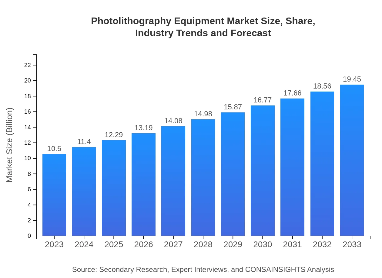
| 2023 Market Size | $10.50 Billion |
| CAGR (2023-2033) | 6.2% |
| 2033 Market Size | $19.45 Billion |
| Top Companies | ASML , Nikon Corporation, Canon Inc., Ultratech (acquired by Veeco Instruments Inc.) |
| Last Modified Date | 31 January 2026 |
Photolithography Equipment Market Overview
Customize Photolithography Equipment Market Report market research report
- ✔ Get in-depth analysis of Photolithography Equipment market size, growth, and forecasts.
- ✔ Understand Photolithography Equipment's regional dynamics and industry-specific trends.
- ✔ Identify potential applications, end-user demand, and growth segments in Photolithography Equipment
What is the Market Size & CAGR of Photolithography Equipment market in 2023?
Photolithography Equipment Industry Analysis
Photolithography Equipment Market Segmentation and Scope
Tell us your focus area and get a customized research report.
Photolithography Equipment Market Analysis Report by Region
Europe Photolithography Equipment Market Report:
The European market is estimated at $3.65 billion in 2023 and poised to grow to $6.77 billion by 2033. Europe’s focus on technological sovereignty and sustainability in semiconductor manufacturing fosters a favorable environment for photolithography equipment market growth.Asia Pacific Photolithography Equipment Market Report:
The Asia-Pacific region, valued at $1.79 billion in 2023, is projected to grow significantly, reaching approximately $3.31 billion by 2033. The growth is primarily driven by countries like China, Japan, and South Korea, which are leading semiconductor manufacturing hubs. The increasing investments in R&D and the presence of major semiconductor suppliers contribute to this region's dominant market position.North America Photolithography Equipment Market Report:
North America, valued at $3.49 billion in 2023, will see growth to $6.47 billion by 2033. The U.S. is home to major semiconductor companies and R&D facilities, which is expected to bolster demand for advanced lithography technologies, particularly in AI and high-performance computing sectors.South America Photolithography Equipment Market Report:
In South America, the market is relatively smaller, valued at $0.67 billion in 2023 and expected to grow to $1.24 billion by 2033. The growth in this region is driven by ongoing industrialization and the expansion of electronic manufacturing services, though it remains subject to economic fluctuations.Middle East & Africa Photolithography Equipment Market Report:
The market in the Middle East and Africa is anticipated to grow from $0.89 billion in 2023 to $1.66 billion in 2033, fueled by increasing investments in electronics manufacturing and technology-driven initiatives across the region.Tell us your focus area and get a customized research report.
Photolithography Equipment Market Analysis By Technology
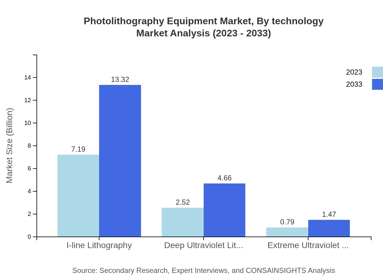
The market analysis by technology reveals significant growth, particularly in the EUV segment, which is expected to capture a larger share of the market due to its capabilities in producing advanced microchips. I-line and DUV technologies continue to play critical roles in the manufacturing of less complex devices but face competition from EUV advancements.
Photolithography Equipment Market Analysis By Application

The application analysis indicates that semiconductor manufacturing leads the market, with a growing share of approximately 68.48% in 2023. Consumer electronics and telecommunications also significantly contribute, benefiting from the rise in portable electronic devices and the 5G rollout.
Photolithography Equipment Market Analysis By End User

Key end-users for photolithography equipment include semiconductor manufacturers and consumer electronics companies. This segment is vital for producing advanced devices and components, driving steady demand for innovative photolithography solutions.
Photolithography Equipment Market Analysis By Innovation

Innovations such as improved optical systems and automation integration are transforming the photolithography equipment market. Companies are focusing on enhancing throughput while maintaining precision to meet the industry's growing demands.
Photolithography Equipment Market Trends and Future Forecast
Tell us your focus area and get a customized research report.
Global Market Leaders and Top Companies in Photolithography Equipment Industry
ASML :
ASML is a leading provider of photolithography equipment, particularly known for its EUV lithography systems that enable advanced semiconductor fabrication.Nikon Corporation:
Nikon is recognized for its high-precision lithography systems, specializing in both DUV and immersion lithography technologies, serving global semiconductor manufacturers.Canon Inc.:
Canon offers a range of lithography equipment and is involved in developing innovative solutions for the semiconductor manufacturing process.Ultratech (acquired by Veeco Instruments Inc.):
Specialized in advanced packaging and lithography equipment for the semiconductor market, Ultratech provides solutions that enhance manufacturing efficiency.We're grateful to work with incredible clients.


FAQs
What is the market size of photolithography equipment?
The photolithography equipment market is valued at approximately $10.5 billion in 2023, with a projected CAGR of 6.2% leading to significant market growth by 2033.
What are the key market players or companies in the photolithography equipment industry?
Key players in the photolithography equipment market include ASML Holding N.V., Nikon Corporation, and Canon Inc., which dominate the market with their advanced technological offerings and strong financial performance.
What are the primary factors driving the growth in the photolithography equipment industry?
Growth drivers include increasing demand for semiconductor devices, advancements in lithography technologies, and the expansion of applications in consumer electronics and telecommunications.
Which region is the fastest Growing in the photolithography equipment market?
Asia-Pacific is emerging as the fastest-growing region in the photolithography equipment market, with growth anticipated from $1.79 billion in 2023 to $3.31 billion in 2033.
Does ConsaInsights provide customized market report data for the photolithography equipment industry?
Yes, ConsaInsights offers customized market report data tailored to the unique needs of stakeholders in the photolithography equipment market, ensuring relevant insights.
What deliverables can I expect from this photolithography equipment market research project?
Deliverables include comprehensive market analysis reports, regional forecasts, competitive landscape assessments, and segmented market insights covering various technologies and applications.
What are the market trends of photolithography equipment?
Current trends involve the shift towards advanced lithography techniques such as EUV, a rise in automation, and growing investment in R&D to enhance semiconductor manufacturing capabilities.